Phototooling: Enabling rapid & cost-efficient precision manufacturing
Phototooling plays a crucial role in the photochemical etching process. This article explores what phototooling is and how it is utilised while highlighting the benefits it offers compared to traditional sheet metal machining processes including stamping and laser cutting.
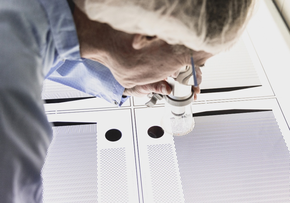
What is a photo tool?
A photo tool is used to transfer the computer-aided design (CAD) image of a component design onto sheet metal before prototype or series production using the chemical etching process.
The process of creating the photo tool starts with the initial design, which is generated using CAD software. This design is subsequently compensated to account for variations in the etching process before being printed or ‘plotted’ onto mylar sheets.
These mylar photo tools can be single or double-sided, with double-sided variants employed for more intricate geometries or when etched features are required on both sides of the metal sheet.
How does phototooling work?
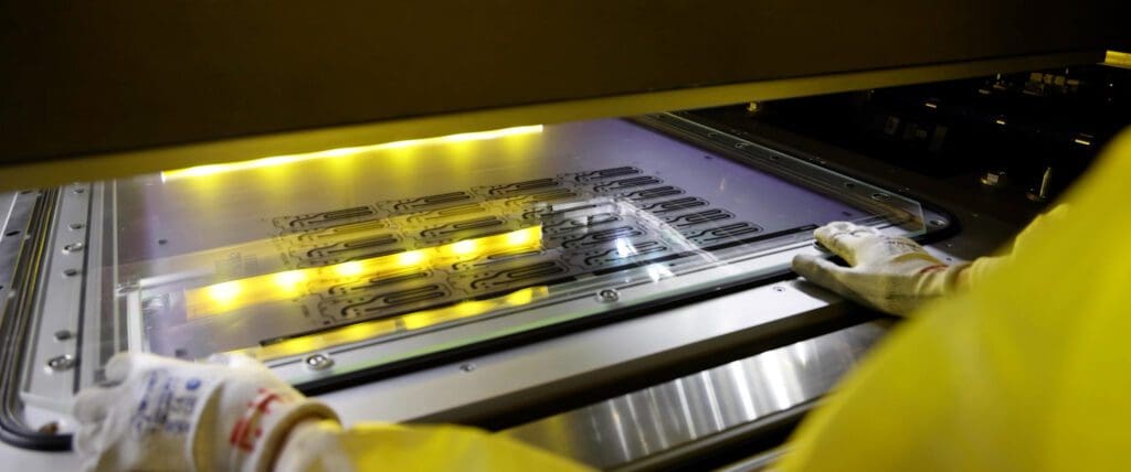
Phototooling functions as a stencil when paired with a metal sheet coated with a photosensitive material. The photoresist undergoes a controlled reaction upon exposure to ultraviolet light through the photo tool, imprinting the desired design onto the substrate material. Subsequently, the material undergoes chemical treatment to develop and expose the desired pattern through the photoresist before etching—a subtractive process that utilises chemical etchants to selectively dissolve the exposed sheet metal.
How does phototooling compare to traditional sheet metal machining tooling?
Stamping
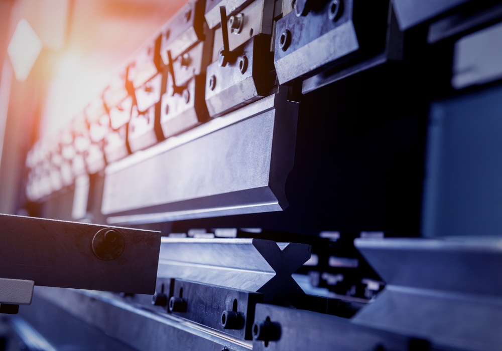
In the stamping process, a toolmaker designs a set of specialised punches and dies, which are then meticulously machined according to detailed blueprints.
The production of stamping tooling can be quite costly, often reaching tens of thousands of dollars, depending on factors like component complexity, size and the materials selected. Lead times can also fluctuate from weeks to months, impacted by the intricacies of the tooling.
Furthermore, challenges may arise in the maintenance of stamping tooling due to wear and tear, leading to increased expenses and prolonged lead times.
Phototooling versus stamping tooling
Phototooling provides a cost-effective alternative to traditional hard stamping tooling. Printing the tooling directly from CAD data enables its rapid creation, making modifications simpler and expediting lead times. Digitally produced phototooling, usually priced around $200, also offers economical prototyping. Additionally, its mylar sheets are durable, easily interchangeable and reusable, further reducing costs and lead times.
Laser cutting & water jet cutting
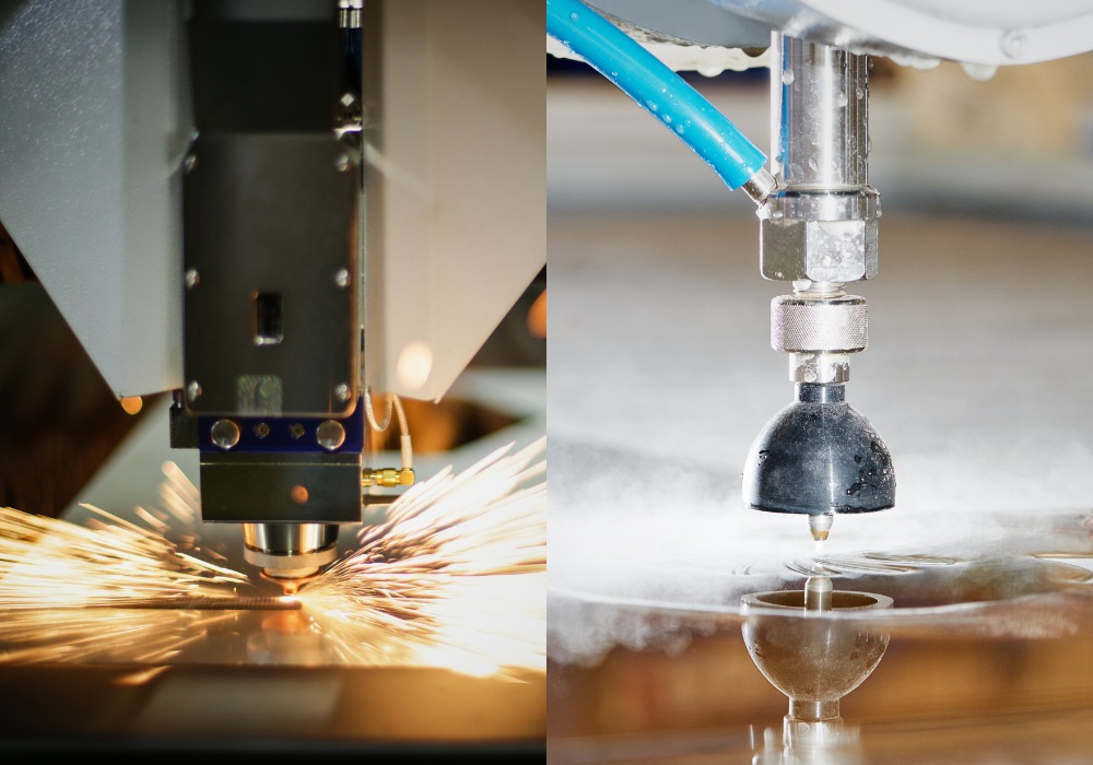
Laser cutting and water jet cutting share a common feature: they both remove the necessity for physical hard or soft tooling. Instead, a laser or water jet is programmed to precisely cut desired components from a metal sheet. By eliminating the need for tooling, the primary expenditure is restricted to the programming charge, rendering the setup for both processes cost-efficient for engineers.
Nevertheless, notwithstanding their affordability, the setup represents only the initial phase of the process. As single-point processes, lead times can stretch to several weeks, and additional challenges may emerge when machining intricate components that demand high levels of accuracy.
Phototooling versus laser cutting & water jet cutting tooling
While phototooling necessitates a modest financial investment, it stands out for its ability to accommodate intricate designs with unmatched precision, allowing for design adjustments until component specifications are fulfilled. Additionally, chemical etching eliminates the risk of burrs and stresses, ensuring optimal efficiency of components.
Electroforming
Electroforming, a technique involving the deposition of metal onto a conductive surface through electrolysis, employs various forms of tooling. For instance, glass tooling operates similarly to mylar sheets utilised in chemical etching or laser direct imaging (LDI). In LDI, the CAD design is transferred onto a substrate’s photoresist-coated surface using a laser. This tooling allows engineers to achieve precision up to ±1 micron, offering ultrafine detail and tight tolerances surpassing other sheet metal machining technologies.
Despite its unparalleled accuracy and precision, electroforming stands out as the most expensive machining process. Traditional electroforming tooling typically incurs costs in the thousands of dollars, and programming expenses must also be factored in when employing LDI. Additionally, electroforming presents limited material flexibility, usually confined to copper and nickel.
Phototooling versus electroforming tooling
While not reaching the precision levels of electroforming, phototooling presents a more cost-friendly alternative. It grants engineers the ability to partially etch components by positioning two distinct photo tools on opposing sides of the substrate, resulting in an ‘engraved’ feature. Moreover, chemical etching demonstrates exceptional versatility by accommodating over 2,000 types of material variants, thereby providing engineers with a wide and adaptable material selection for their precision component design.
Conclusion
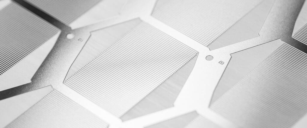
Phototooling emerges as a versatile method for producing precision-etched components. Employing wear-resistant mylar sheets contributes to cost and lead time reductions, making phototooling a cost-effective option. Design engineers also enjoy unparalleled freedom and flexibility, as it eliminates additional alteration costs associated with hard tooling. Furthermore, phototooling excels in managing complex and intricate designs, ensuring precision and uniformity across various applications and industries.
Chemical Etching Whitepaper
Learn how chemical etching can overcome the limitations of traditional sheet metal machining technologies.
Download